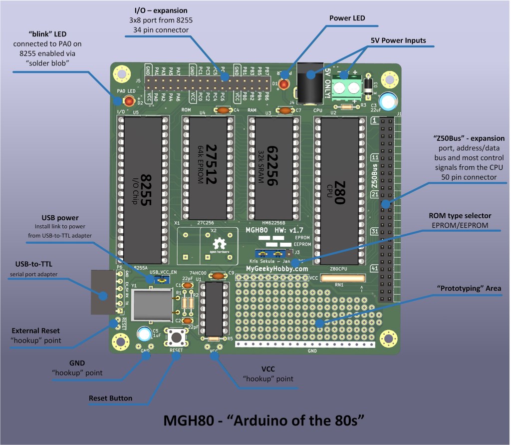
A few years ago, I shared a Z80 “single board computer” design called MGH80… it was meant to be a bit of an “Arduino of the 80s” / “simple Z80 experiment platform”… I finally had a chance to complete the project. In this post, I’ll share some of the design aspects and implementation details.
The project actually came from my desire to experiment with the Z80 CPU. I wasn’t planning anything specific, and I didn’t want to “lock” myself into any implementation… A lot of my Z80 experiments share common sections… and what I wanted to avoid is “breadboarding” hundreds of wires every time I’m working on a new design. So this new design/PCB was supposed to cover 90% of the common connections, leaving enough flexibility to implement some of the specifics per design… Think about it… there is only one way to connect the Z80 CPU data line zero to the external memory data line zero 🙂 … in fact, most of the data and address line connections are made in a “standard” way to typical SBC peripherals… With all this flexibility, I also wanted the “base” design to be complete enough to “blink an LED”… or even a bit more 🙂
Let’s look at some of the components of the design
Main CPU
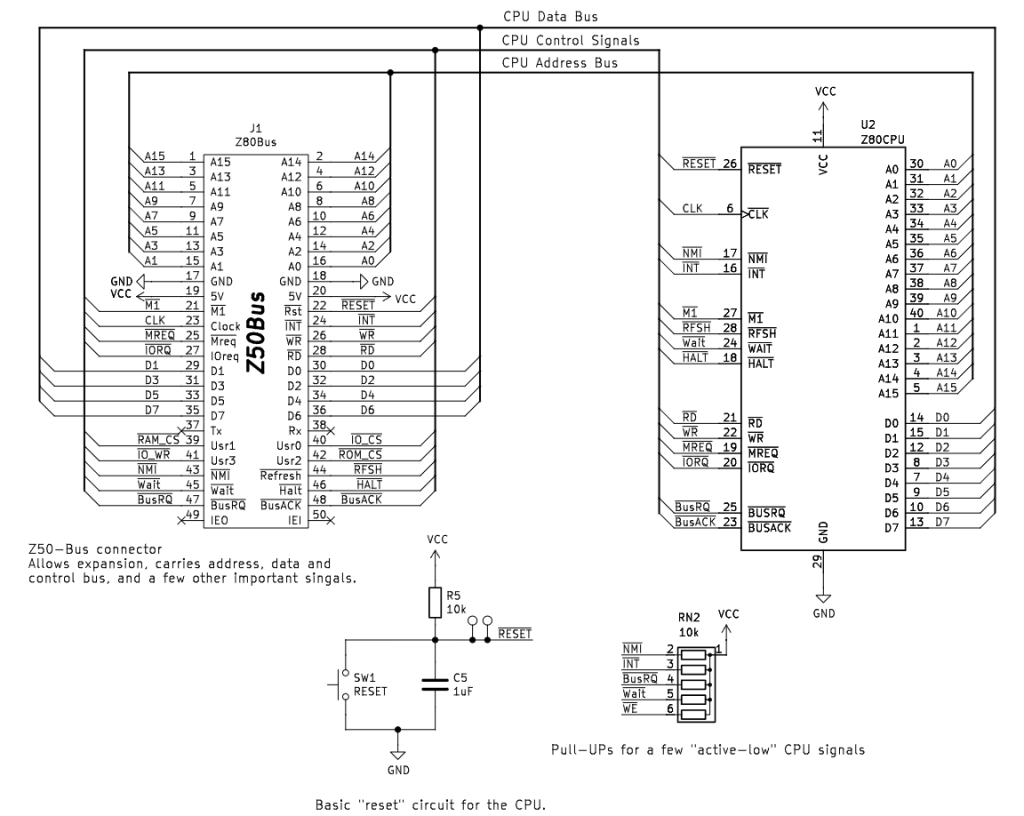
This is a very simple way to “wire” the CPU … Signals from the CPU feed the relevant “bus”. Almost all CPU signals are extended to the Z50Bus expansion connector J1… This is a “standard” Z80 expansion bus, as documented here. I tried to follow the specification as described on LiNC website.
This section also contains a very simple “reset” circuit … just a push button, small electrolytic capacitor, and a resistor…
Lastly, this section also contains a pull-up resistor pack to keep some of the “active-low” signals on the CPU disabled by default.
Memory
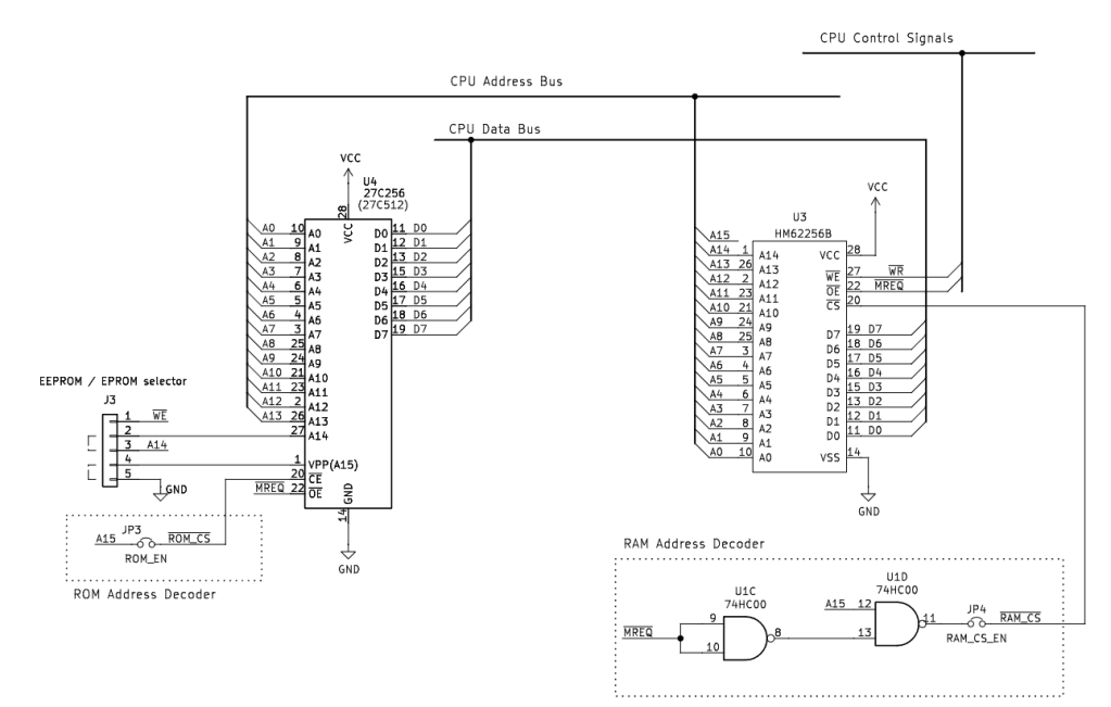
The memory system supports a single 32Kb EPROM (or EEPROM memory selected via jumpers J3), a single 32kb RAM chip. You can use 27256 or 27512 chips, but only the first 32Kb of the memory is supported. Those two chips are supported by a very simple “address” decoder circuit… for RAM, we use A15 and /MREQ to enable RAM for addresses starting at 8000h. For ROM, we use the A15 signal to enable ROM only for address ranges 0000h to 7FFFh; additionally, we run /MREQ directly to the ROM chip to enable the chip for memory access only.
Input / Output
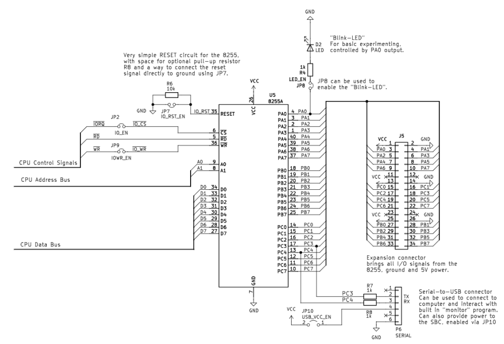
The Z80 CPU has a dedicated I/O chip in the format of the PIO … but since I’m very familiar with the 8255 I/O chip, I decided to use it instead… The address decoding logic is super simple (but has some drawbacks as a result). We map the CPUs /IORQ signal directly to the 8255 /CS, the CPU’s /RD to 8255 /RD, and CPU’s /WR to 8255 /WR. This usually works … some 8255s are “picky” with timing and may not support this simplified address decoder (8255 without any dashes in the part worked best for me … so avoid 8255-2 or 8255-5 … just plain 8255).
The 8255 also serves two other important functions – our “Blink LED” connected to PA0 (can be disabled via JP8) … and our “software” “bit-bangged” serial port signals “TX” connected to PC3 and “RX” connected to PC4 … RX, TX ground and power is connected to connector P6 where you can install USB-to-TTL serial adapter and interact with built in “monitor” or “BASIC”.
Clock
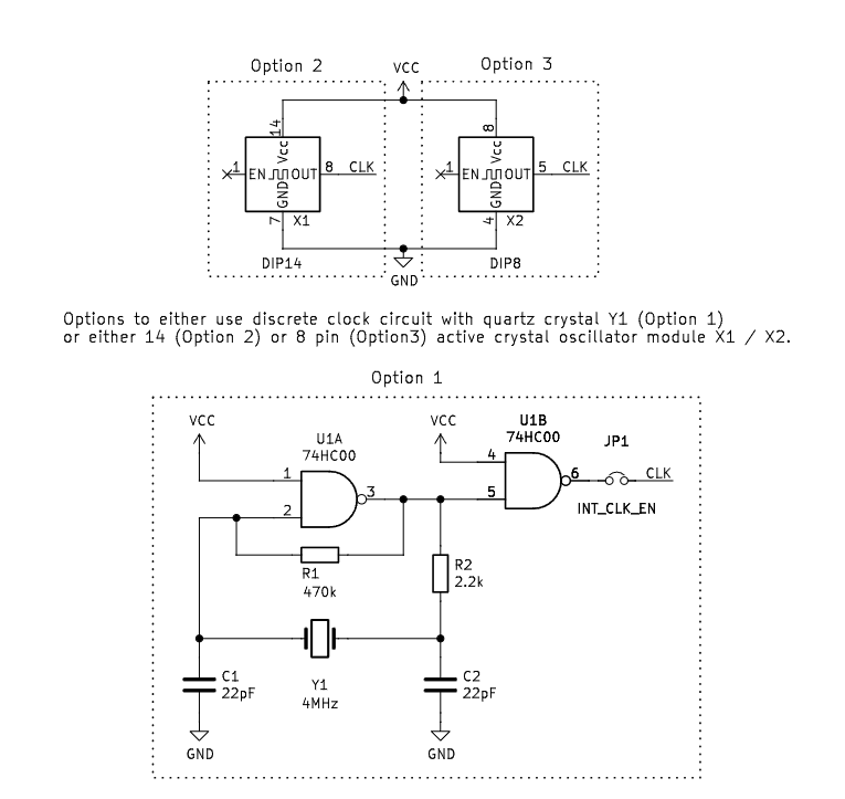
Our Z80 CPU needs an external clock signal… this can be provided via a discrete circuit with a crystal resonator Y1 or via an active oscillator module X1/X2.
Power
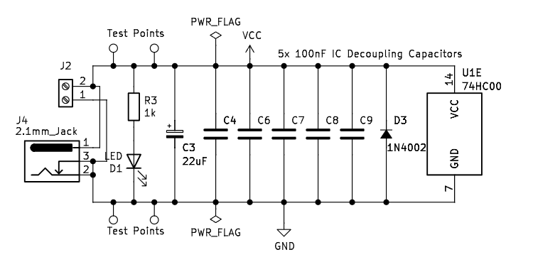
The last section deals with standard “decoupling” capacitors, power inputs (via barrel jack or terminal block), and a “POWER on LED.”
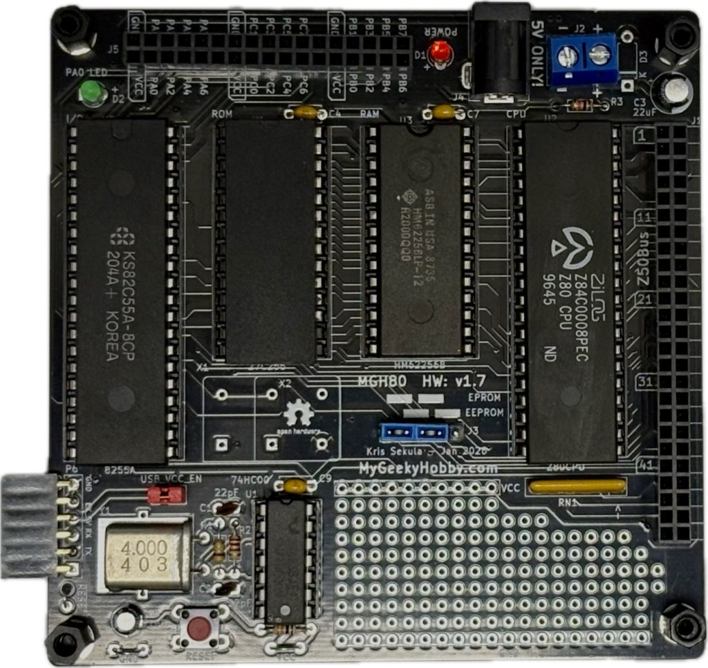
The “MGH80 PCB” v1.7
The “MGH80 PCB”
The full schematic is available on GitHub; the resulting PCB is presented here. I added “experiments” / “prototyping” area in case you want to add some missing features or implement a more “sophisticated” address decoding for memory or the I/O.
This project has been supported by PCBWay. I highly recommend their PCB prototyping services. If you plan to order PCBs, take the opportunity to support my projects by signing up to PCBWay using my referral link:

(This will give me a few $ credit for my next project, and you will also get a few $ towards your order in return)…
Once you sign up to PCBway, order the project PCB using this link:
Here is how the final “real” PCB looks after assembly