
In my Commodore 64 Power Supply magic post, I talked about the internal power supply and how not everything that you see when you quickly glance is as obvious as it seems. Yet again I’m faced with a similar situation. I needed an external power supply for one of the machines that I purchased recently, and I didn’t want to pay almost the equivalent of half of the cost of the computer for a new power supply. I searched eBay and come across a “faulty, for parts” unit. Perfect for me, as I’ve got a small “lab” at home and I’m able to troubleshoot and hopefully fix it. It was the 902503-02 part number, that as opposed to some of the “newer” version is not “potted” and can be opened and inspected. Before the auction was over I was “researching” the power supply. My “research” started with googling “902503-02 schematic diagram”. The result brings a few similarly looking diagrams, but here is one of the first hits that I found:
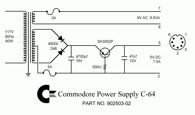
Well, to me it doesn’t look like the original schematic diagram, it’s more of a reverse engineered diagram that someone has created looking at the real circuit of the power supply. We know roughly what to expect on the basis of what I covered in my previous post – two separate outputs: one is unregulated 9V AC, and regulated 5V DC. And at first glance, it sort of looks ok but in reality, this “diagram” is seriously misleading! Here is what I’ve noticed:
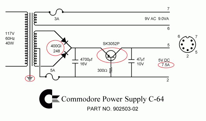
Let’s do the “simple” ones first: the diodes have some strange part numbers, in fact, those should be marked 1N5400. The “ground” symbol from the transformer goes nowhere, as there is only one of them. One of the outputs is marked 7.5A … 7.5A!!?? This should be corrected to 7.5VA – alternatively, the entire thing could be just marked 5V/1.5A. But the biggest and a major mistake is the “transistor” marked SK3052P. Yes, it’s a 3 legged device in a “TO-3P package” that looks like a transistor, but it would be impossible to create a 5V regulator based on a single transistor and a resistor. In fact, the “SK” in the part number is a logo for a Japanese company called “Sanken”, the full part number is “SI-3052P” – a 5V at 2A linear voltage regulator integrated circuit. So the author has done the following “mind shortcut”:

This is very unfortunate “shortcut” as I’ve seen a few posts on C64 forums where people are referring to that regulator as “transistor”! Well now you know it’s not, and the SI-3052P provides a few important functions: it regulates the output voltage at 5V DC independent of the load and it has a built-in overcurrent protection that will “kick in” when the load exceeds around 2.4A. Based on this new information and after “inspecting” one of those power supplies, I’ve re-created the diagram adding a few more details:
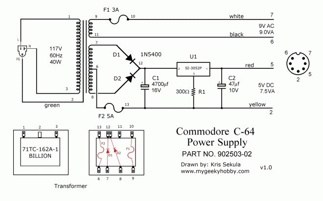
here is full resolution picture
Let me quickly describe what happens: mains voltage is supplied to the primary winding of our power transformer, notice the “protective earth” pin is somehow connected to the transformer (looks like it goes in the layer between the primary and secondary winding) but it doesn’t extend to the output and is not connected to the computer at all. There are two secondary windings:
- Pin 9 and 11: provides 9V AC that goes directly to the output. Its protected by a 3A fuse F1, I’ve marked the voltage rating of the fuse (250V) but this is not as important on the secondary side, what is important is to know if this fuse is a “slow” or “fast” acting fuse. Unfortunately, the fuse itself doesn’t have any markings saying what type of fuse it is. Inspecting it physically and considering its function I think it’s a “fast” acting fuse. You may ask why do we need this fuse, isn’t there another fuse inside the C64 that is on the 9V AC power rail. It’s true but the fuse here inside the power supply is supposed to protect the transformer form accidental shortcuts on the output before the power supply is even plugged into the computer.
- Pin 7 and 8: provides 18V AC with a “center” tab on pin 6. This center pin allows the use of two diodes in a full wave rectifier configuration, saving cost by not having to use a 4 diode full bridge rectifier configuration. Next follows a large smoothing filter capacitor C1. This part of the circuit is protected by 5A fuse F2, yet again there is no marking on the fuse, but considering it has to withstand a larger than standard operating conditions initial charging current of the smoothing capacitor and a clearly different physical appearance I deduct it’s the “slow” acting fuse type.
The unregulated voltage from C1 is regulated using U1, the SI-3052P integrated circuit. On the output of U1 we see an additional small electrolytic capacitor C2, that is recommended by the manufacturer to prevent oscillation. There is one more component, the 300 Ohm resistor R1, it’s used to “raise” the output voltage a bit over the nominal 5V to compensate for the losses on the long wires between the power supply and the computer. This is actually very surprising, as looking at the U1 datasheet, we see Note 3: “The output voltage may not be adjusted by raising the ground voltage (using a diode or resistor)”. This is related to the built-in “foldback overcurrent protection circuit” that will be affected if pin 3 of U1 is not at “ground level”. Looks like the engineers designing the power supply ignored the note. When I get a chance I will try to test and compare the behavior of the power supply in a fault condition, with and without that resistor.
Quick comment on the construction of the power supply. The diodes and fuses are soldered directly to the transformer “pins” (with the help of some additional internally unconnected pins 10 and 12). The rest of the components are mounted on a small printed circuit board (PCB). The transformer and the PCB are marked “Billion”, and I assume this is “contract” manufacturer Billion Electric Co., Ltd. of Taiwan, that Commodore tasked with the creation of this power supply.
Lastly, one should note this is a linear power supply, cheap but very inefficient. At full load (C64 plus accessories plugged into the expansion port drawing in total around 1.4), the input voltage on U1 is over 10V, so to “drop” the voltage to 5V on the output the linear regulator has to dissipate close to 8W of power (voltage on input minus voltage on output multiplied by current). U1 and its heatsink get extremely hot, and as we know, hot semiconductors don’t last long…
In part 2, I will cover the restoration/repair of my eBay purchased power supply, I will share some test results and implement few improvements… stay tuned.


